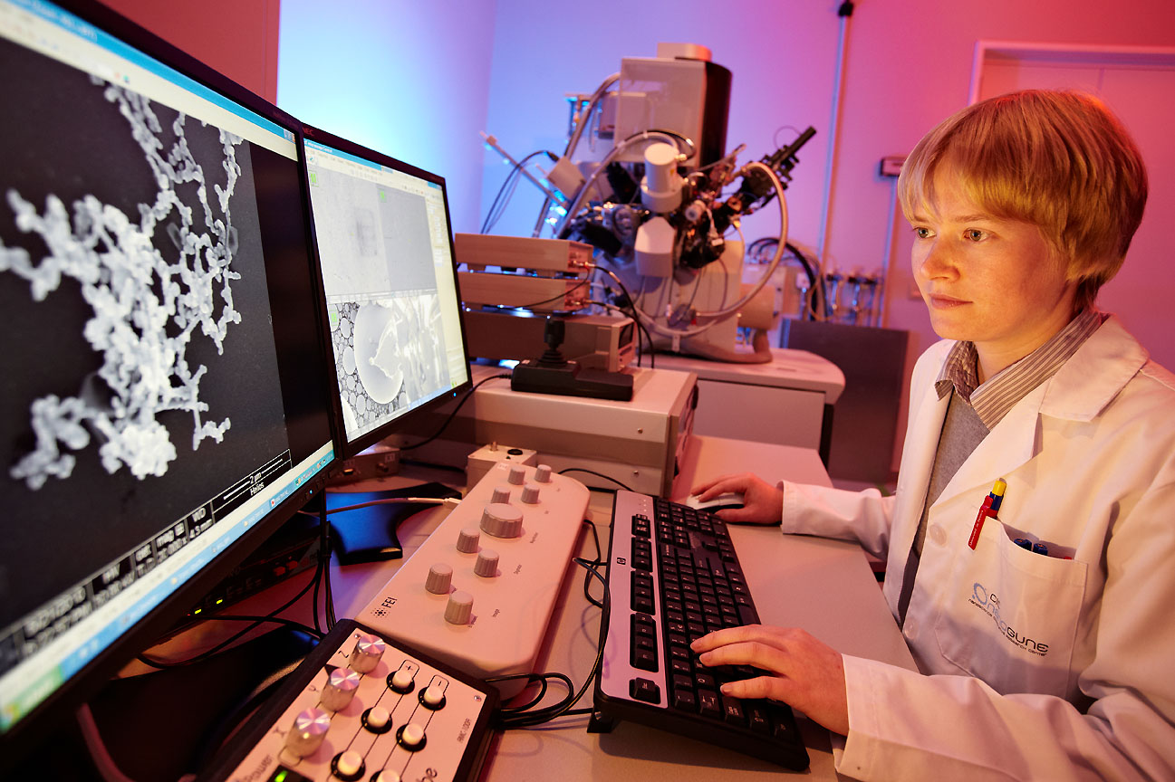
Dual-beam FIB/SEM (Focused Ion Beam and Induced deposition)
What we can offer (with the system):
- High resolution SEM imaging.
- Focused Ion Beam and Focused electron beam induced deposition (FE(I)BID) of W, Au, Co, Pt and SiOx.
- Surface patterning by FIB with a minimum feature size of 10 nm (processing areas below mm2).
- Complex structures fabrication (including 3D structure).
- Sample preparation for transmission electron microscopy (TEM).
- 3D characterization of the structure with FIB Nano tomography. Imaging of large areas up to cm2
- Micro and nano structure fabrication
Possibility to fabricate:
- Etching or deposition of different structures: high resolution nanopatterns, direct fabrication of photonic crystals, micro/nanopillars arrays, fabrication of modification/tuning of AFM cantilevers, sharp probes for SNOM, diffractive optical elements, micro/nano labelling, conductive bridges between contacts…
- Micro and nano structures and devices on different substrates (glass, silicon, CaF2)
- Customized structured calibration and reference samples (microscopy, metrology).
- Topographically changed surfaces with advanced properties (optical, mechanical, adhesion, friction).
Interesting for (with the system):
Material science, microelectronics and semiconductors, automotive, laboratory test facilities, microscopy laboratories, machine tool manufacturers, iron and steel industry, energy storage and solar energy materials industry, objects of cultural heritage examination, energy and petrochemical companies.
Tags
Focused ion beam (FIB)
deposition
nanofabrication
nanopatterns
ion milling
TEM sample preparation
3D structuresPhysical etching and sputtering
nanodevices
calibration samples