Environmental Scanning-electron Microscope (eSEM-FEI Quanta 250)

Scanning electron Microscopy (SEM)/(ESEM)
Environmental Scanning-electron photograph

What we can offer (with the system):

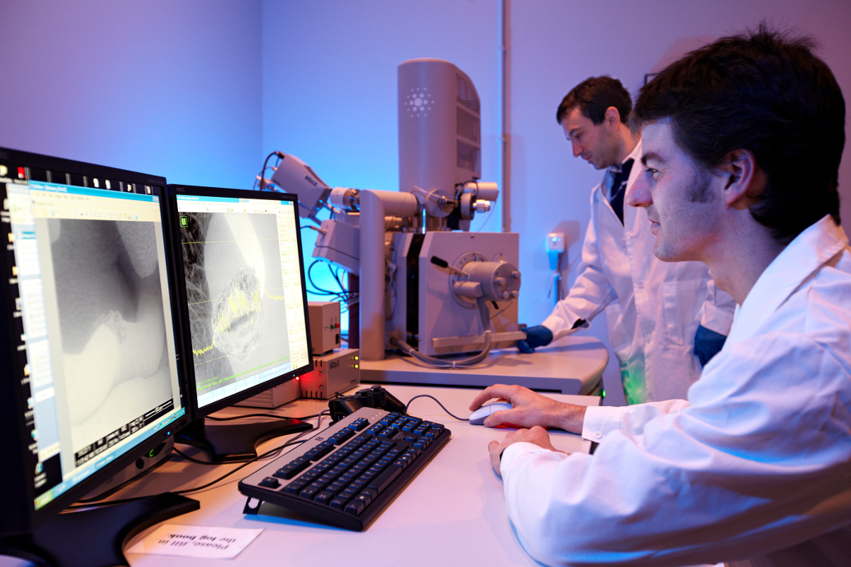
  • SEM – morphological surface analysis

  • STEM (Scanning Transmission Electron Microscopy) – resolution < 1 nm at 30 kV

  • ESEM – non conducting samples without any coating Imaging of wet samples and liquid water

  • Cryogenic cooling stage

  • Possibility to inject liquid by manipulators while imaging

  • In-situ electrical measurements – 3 probes, probing current 10 nA to 100 mA, probing max. voltage 100 V and probing resistance 7 Ω

  • Extra-large high-resolution surface imaging (up to cm2 areas with nm resolution)

  • EDX – Energy dispersive x-ray spectroscopy

  • In-situ force measurement system

Possibility to fabricate (with the system):

Interesting for (with the system):

Material science, microelectronics and semiconductors, automotive, laboratory test facilities, microscopy laboratories, machine tool manufacturers, iron and steel industry, life science, objects of cultural heritage examination, energy and petrochemical companies

Tags
Scanning Electron Microscopy; SEM; Environmental; ESEM; In situ; Surface analysis; Chemical analysis; EDX;

Do you want more information?

datos
question
bottom

Anti spam: Write the result of adding eight and the number six in letters

Basic information on data protection
Data controller ASOCIACIÓN CENTRO DE INVESTIGACIÓN COOPERATIVA EN NANOCIENCIAS – CIC nanoGUNE
Purposes Process and manage your information request.
Rights You have the right to withdraw your consent at any time, oppose their processing, access, rectify and erase the data, in addition to other rights, by writing to CIC nanoGUNE via post or to the email address nano@nanogune.eu.
Additional information You can consult additional, detailed information on Data Protection in the Privacy Policy section.
By clicking on “Submit” I consent to the processing of my data under the terms indicated