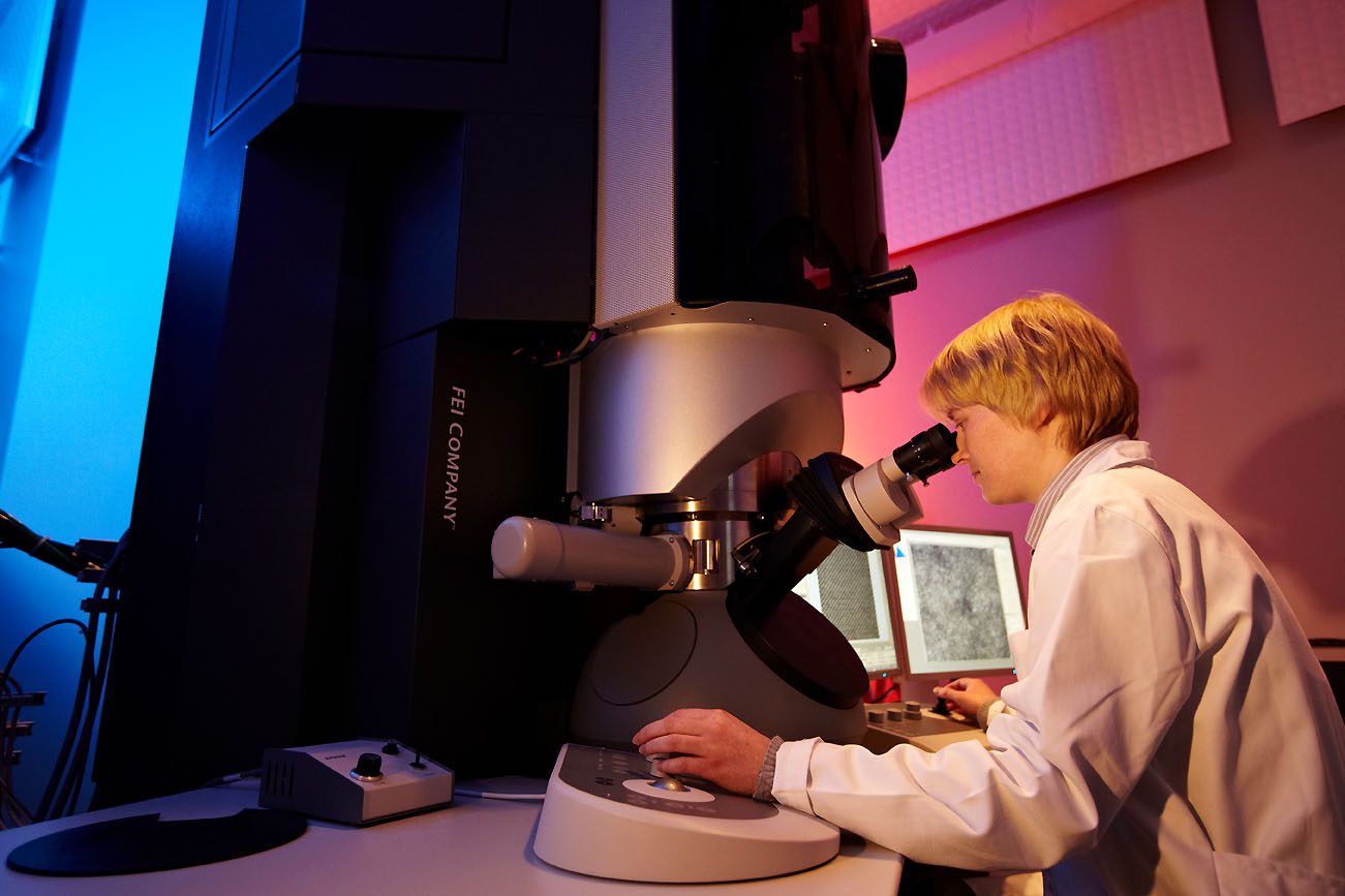
High-resolution Transmission Electron Microscope (HRTEM)
What we can offer (with the system):
- High resolution TEM/STEM imaging of crystalline or amorphous materials
- Atomic structure of 2D materials
- Structure of interfaces and grain boundaries, defects, nanoparticles
- Nanostructural analysis of thin films, layers, multilayers and interfaces
- Characterization of magnetic nanomaterials: thin films, nanowires, nanoparticles
- Chemical elements local analysis or mapping; bonding state and valence state characterization
- 3D characterization of materials by means of electron tomography
- Cooling/Heating (-170C to 1200C) while imaging with TEM/STEM
Interesting for (with the system):
Material science, microelectronics and semiconductors, automotive, laboratory test facilities, microscopy laboratories, machine tool manufacturers, iron and steel industry, life science, objects of cultural heritage examination, energy and petrochemical companies
Tags
Transmission Electron Microscopy; TEM; STEM; TEM/EDX; EELS; in situ; Lorentz; Holography; aberration corrector; high resolution