SPECTER - Spin-charge conversion in highly resistive spin-orbit materials

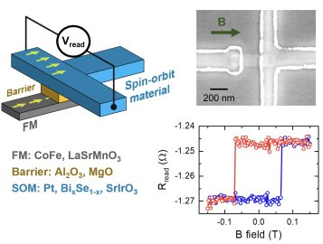
With the current technology of transistors reaching characteristic sizes of a few nanometers, and heating effects becoming more severe, the regular functionality of processors is at stake. In the next few years, new technologies are required to sustain the increasingly high demands imposed by the consumer electronics industry worldwide. Among the wide range of proposed options, spintronics is considered to be one of the leading candidates to fill this gap, backed by recent proposals for spin-based computation using magnetoelectric spin-orbit devices. In these devices, the magnetic state of a ferromagnetic material is read through the conversion of spin currents in charge currents, where two resistance levels can be unambiguously detected depending on the magnetization direction of the ferromagnet, i.e. a “1” and a ”0” state.
The main goal of SPECTER is to find the most suitable material exhibiting large spin-to-charge conversion efficiencies combined with large resistivities, allowing the generation of high output voltages for a subsequent writing step. To achieve this result, a careful balance between adequate materials beyond the conventional high spin-orbit coupling metals, and device fabrication of nanostructures that maximize spin-to-charge conversion detection needs to be achieved. With this proposal, we want to explore nanostructured topological insulators and correlated oxides fabricated by industry-friendly techniques, such as sputtering and e-beam lithography, while benchmarking them for future spin-based devices. This way, SPECTER not only poses a revolutionary step towards the next generation of processors, but also aims at acquiring scientific knowledge with technological applications to be useful for both academia and industry. Moreover, the ultimate goal of SPECTER is to offer high-quality interdisciplinary research training for an aspiring young researcher helping him to build a promising scientific research career.

Disclaimer: The contents included in the present website reflect only the author’s view and the Research Executive Agency (European Commission) is not responsible for any use that may be made of the information it contains.
