Teaching the world about cutting-edge tools for nanoscale optical imaging
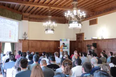
“When we developed the near-field optical nanoimaging and nanospectroscopy tools, which we named s-SNOM and nano-FTIR, I never thought that they could have such wide application potential”, says Ikerbasque Research Professor Rainer Hillenbrand when asked about the evolution of his field of research. This week, from 6 to 9th June, we welcome about 70 researchers eager to learn how to get the most out of the techniques, because San Sebastian hosts the Near-fiel Optical Nanoscopy Summer School, organized by CIC nanoGUNE, Ensemble 3 and Attocube.

s-SNOM and nano-FTIR are unique optical imaging and spectroscopy tools that enable nanoscale imaging and spectroscopy in a broad spectral range, between visible and terahertz frequencies. Rainer Hillenbrand was one of the researchers involved in the development of these techniques and their commercialization, opening a completely new field of experimental research of optical phenomena and materials properties at the nanoscale. Since he joined nanoGUNE in 2009, his group has been further developing and applying these tools for exploring novel materials and light-related phenomena on the nanometer scale.
“It is really exciting to see how a technique you have developed can revolutionize the nanoscale analysis of materials”, expresses Hillenbrand. For example, s-SNOM led to major breakthroughs in understanding of how light and other forms of electromagnetic radiation propagate on 2D materials, such as graphene. “We have been able to ‘squeeze light’ so that it fits into these nanosized materials and visualized how it behaves there, opening new possibilities for the development of optoelectronic devices for detector, communication or sensor applications”, explains the researcher.
Furthermore, the s-SNOM and nano-FTIR instruments can be considered as chemical microscopes for the nanoscale. This makes them very interesting tools for the field of materials science. They allow for analyzing drugs, pharma products, semiconductors, contaminations, corrosion of materials and to study catalysis. Nowadays, it is starting slowly to be used in industrial R&D for studying proof-of-concepts, for failure analysis in chip manufacturing, or for analysis of pharmaceutical and cosmetic products.
“The potential of this technology is generating great interest in research and development groups around the world, and it is for this reason that we took on the challenge of organizing this first school. We have been able to combine specific sessions to teach the fundamentals and practical aspects of the technique, instrumentation, methodology, and data analysis, with talks on the latest developments in the field by international experts”, adds Hillenbrand.
There is still a lot of room for further developments. The following challenges according to Hillenbrand are: the imaging in liquids in order to analyze “in-vivo” samples; imaging of ultra-fast processes to get a better understanding of physical and chemical processes; and optical imaging at low temperature to study fundamental phenomena in quantum materials. The development of these new capabilities will further expand unique application potential of s-SNOM and nano-FTIR spectroscopy.
