Related news by tag 2D materials
The Nanodevices group participates in the 2D-INK Fet Open project
The Nanodevices group at nanoGUNE is one of the 9 partners of the project. Its contribution will be to fabricate and test transistors with the semiconductor ink provided by other partners in the consortium. NanoGUNE will also take care of the miniaturization of the devices, having in mind possible electronic applications, such as wearables. With this purpose, they will receive 297,600€ for a 3 years period.
The company Graphenea, launched by nanoGUNE and a group of private investors in 2010, will also participate in the project. The collaborative research-team is completed by six more European university partners: Algoritmi Center of the Universidade do Minho (Braga, Portugal); ICMol Institute of the Universitat de Valencia (Valencia, Spain); the Technische Universität München (Munich, Germany); the Katholieke Universiteit Leuven (Leuven, Belgium); the Universität Wien (Vienna, Austria); and the University of Nottingham (United Kingdom).
The FET-OPEN (Future and Emerging Technologies) projects of the European Union support research lines in early stages, based on ideas that may arise new technology lines. Thus, the EU initiative encourages scientists and engineers from many disciplines to cooperate in research projects that promote scientific progress. It is noteworthy, too, that the European program FET -OPEN is a highly competitive call: only 24 of the 643 submitted projects (3.7%) have been funded across Europe.
Patents
The development of semiconductor inks from two-dimensional materials with different properties represent, according to the coordinator of the project, Aurelio Mateo-Alonso, "a major breakthrough in the field of new materials for the next generation of ultra-thin electronic devices such as transistors, LEDs, solar cells, protodetectors, etc.". The researchers also predicts the submission of patents, given the technological possibilities of 2D-INK and the involvement of a private company.
Basque researchers turn light upside down
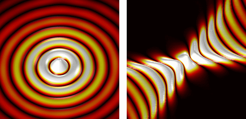
Scientists had already theoretically predicted that specifically structured surfaces can turn the wavefronts of light upside down when it propagates along them. "On such surfaces, called hyberbolic metasurfaces, the waves emitted from a point source propagate only in certain directions and with open (concave) wavefronts", explains Javier Alfaro, PhD student at nanoGUNE and co-author of the paper. These unusual waves are called hyperbolic surface polaritons. Because they propagate only in certain directions, and with wavelengths that are much smaller than that of light in free space or standard waveguides, they could help to miniaturize optical devices for sensing and signal processing.
Now, the researchers developed such a metasurface for infrared light. It is based on boron nitride, a graphene-like 2D material, and was selected because of its capability to manipulate infrared light on extremely small length scales, which could be applied for the development of miniaturized chemical sensors or for heat management in nanoscale optoelectronic devices. On the other hand, the researchers succeeded to directly observe the concave wavefronts with a special optical microscope, which have been elusive so far.
Hyperbolic metasurfaces are challenging to fabricate because an extremely precise structuring on the nanometer scale is required. Irene Dolado, PhD student at nanoGUNE, and Saül Vélez, former postdoctoral researcher at nanoGUNE (now at ETH Zürich) mastered this challenge by electron beam lithography and etching of thin flakes of high-quality boron nitride provided by Kansas State University. "After several optimization steps, we achieved the required precision and obtained grating structures with gap sizes as small as 25 nm”, Dolado says. “The same fabrication methods can also be applied to other materials, which could pave the way to realize artificial metasurface structures with custom-made optical properties”, adds Saül Vélez.
To see how the waves propagate along the metasurface, the researchers used a state-of the-art infrared nanoimaging technique that was pioneered by the nanoptics group at nanoGUNE. They first placed an infrared gold nanorod onto the metasurface. “It plays the role of a stone dropped into water”, says Peining Li. The nanorod concentrates incident infrared light into a tiny spot, which launches waves that then propagate along the metasurface. With the help of a so-called scattering-type scanning near-field microscope (s-SNOM) the researchers imaged the waves. “It was amazing to see the images. They indeed showed the concave curvature of the wavefronts that were propagating away form the gold nanorod, exactly as predicted by theory“, says Rainer Hillenbrand, Ikerbasque Professor at nanoGUNE, who led the work.
The results promise nanostructured 2D materials to become a novel platform for hyberbolic metasurface devices and circuits, and further demonstrate how near-field microscopy can be applied to unveil exotic optical phenomena in anisotropic materials and for verifying new metasurface design principles.
The research has been mainly funded by individual fellowship grants of the European Union Marie Sklodowsca-Curie Actions and the pre-doctoral research grants program of the Basque and Spanish Governments, as well as by the National Science Foundation (USA), and has been carried out in line with nanoGUNEs projects within the EU's Graphene Flagship.
nanoGUNE joins forces with BerriUp and Graphenea to launch the Global Graphene Call
CIC nanoGUNE, BerriUP —a startup accelerator in Donostia— and Graphenea —nanoGUNE’s first startup devoted to the production and commercialization of graphene— have signed a collaboration agreement to drive forward proposals related to research in graphene. So for the first time we are launching the Global Graphene Call designed to develop business ideas linked to graphene.
The participants will need to submit legitimate, in-house projects, and to participate, the project will need to be submitted using the dedicated application form. The starting date for submitting projects is 24 February, 2020 and the deadline is 26 April, 2020.
The shortlisted applicants will be able to take advantage of a programme of customised acceleration at the BerriUp headquarters between June and August 2020, avail themselves of Graphenea material and make use of nanoGUNE’s scientific equipment.