Related news by tag Graphene
II Global Graphene Call, business ideas linked to graphene

In the first call back in 2020, 35 projects were registered and the winning company was Dutch, which underlines the international nature of the call. These results have spurred the launch of this new call in 2022, now with the additional contribution of Fomento San Sebastián.
Unprecedented spin properties revealed in new artificial materials

In conjunction with research staff from the Charles University of Prague and the CFM (CSIC-UPV/EHU) center in San Sebastian, CIC nanoGUNE’s Nanodevices group has designed a new complex material with emerging properties in the field of spintronics.
Repsol and CDTI invest a million euros in nanoGUNE's start-up company, Graphenea
NanoGUNE’s start-up company, Graphenea, has developed innovative technology for the production of high-quality graphene; its products are supplied to 40 countries and to multinationals such as Nokia, Philips and Sigma-Aldrich, amongst others. Graphenea was founded in 2010, in the Basque city of San Sebastian, as a joint venture of private investors and nanoGUNE.
This co-investment, carried out within the remit of the INNVIERTE programme, within the area of new energies, will reinforce technological capacity, will help business growth and, moreover, will enable the company’s international leadership to be maintained within the emerging sector of graphene production. In this sense, the funds will be implemented for accelerating the company’s business plan for industrialisation.
Graphene is a new nanomaterial made up of a single layer of carbon atoms and which has extraordinary optical, electrical, thermal and mechanical properties. This makes it for being in high demand in the development of new disruptive technologies for the storage and generation of energy. Specifically, in this vein, products made from it are employed in making batteries, supercapacitors, solar cell and thermal management devices. Moreover, its materials are also used as polymer or resin additives.
Last year, the world graphene market had a turnover of 6.6 million euros. Analysts estimate that in 2018 this figure will surpass 73 million euros.
3rd Global Graphene Call: international call to promote innovative graphene-based projects

The Basque Nanoscience Research Center, CIC nanoGUNE, together with BerriUp —the number one private startup accelerator in Spain, according to the Financial Times—,
Science: Flatland optics with graphene
Optical circuits and devices could make signal processing and computing much faster. “However, although light is very fast it needs too much space”, explains Rainer Hillenbrand, Ikerbasque Professor at nanoGUNE and the UPV/EHU. In fact, propagating light needs at least the space of half its wavelength, which is much larger than state-of-the-art electronic building blocks in our computers. For that reason, a quest for squeezing light to propagate it through nanoscale materials arises.
The wonder material graphene, a single layer of carbon atoms with extraordinary properties, has been proposed as one solution. The wavelength of light captured by a graphene layer can be strongly shortened by a factor of 10 to 100 compared to light propagating in free space. As a consequence, this light propagating along the graphene layer – called graphene plasmon – requires much less space.
However, transforming light efficiently into graphene plasmons and manipulating them with a compact device has been a major challenge. A team of researchers from nanoGUNE, ICFO and Graphenea – members of the EU Graphene Flagship – now demonstrates that the antenna concept of radio wave technology could be a promising solution. The team shows that a nanoscale metal rod on graphene (acting as an antenna for light) can capture infrared light and transform it into graphene plasmons, analogous to a radio antenna converting radio waves into electromagnetic waves in a metal cable.
“We introduce a versatile platform technology based on resonant optical antennas for launching and controlling of propagating graphene plasmons, which represents an essential step for the development of graphene plasmonic circuits”, says team leader Rainer Hillenbrand. Pablo Alonso-González, who performed the experiments at nanoGUNE, highlights some of the advantages offered by the antenna device: “the excitation of graphene plasmons is purely optical, the device is compact and the phase and wavefronts of the graphene plasmons can be directly controlled by geometrically tailoring the antennas. This is essential to develop applications based on focusing and guiding of light”.
The research team also performed theoretical studies. Alexey Nikitin, Ikerbasque Research Fellow at nanoGUNE, performed the calculations and explains that “according to theory, the operation of our device is very efficient, and all the future technological applications will essentially depend upon fabrication limitations and quality of graphene”.
Based on Nikitin´s calculations, nanoGUNE’s Nanodevices group fabricated gold nanoantennas on graphene provided by Graphenea. The Nanooptics group then used the Neaspec near-field microscope to image how infrared graphene plasmons are launched and propagate along the graphene layer. In the images, the researchers saw that, indeed, waves on graphene propagate away from the antenna, like waves on a water surface when a stone is thrown in.
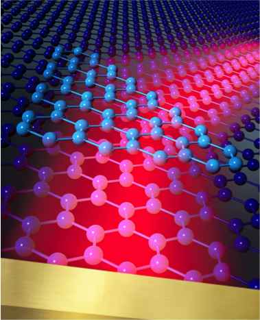
Graphic representation of the refraction of graphene plasmons – launched by a tiny gold antenna – when passing through a one-atom-thick prism
In order to test whether the two-dimensional propagation of light waves along a one-atom-thick carbon layer follow the laws of conventional optics, the researchers tried to focus and refract the waves. For the focusing experiment, they curved the antenna. The images then showed that the graphene plasmons focus away from the antenna, similar to the light beam that is concentrated with a lens or concave mirror.
The team also observed that graphene plasmons refract (bend) when they pass through a prism-shaped graphene bilayer, analogous to the bending of a light beam passing through a glass prism. “The big difference is that the graphene prism is only two atoms thick. It is the thinnest refracting optical prism ever”, says Rainer Hillenbrand. Intriguingly, the graphene plasmons are bent because the conductivity in the two-atom-thick prism is larger than in the surrounding one-atom-thick layer. In the future, such conductivity changes in graphene could be also generated by simple electronic means, allowing for highly efficient electric control of refraction, among others for steering applications.
Altogether, the experiments show that the fundamental and most important principles of conventional optics also apply for graphene plasmons, in other words, squeezed light propagating along a one-atom-thick layer of carbon atoms. Future developments based on these results could lead to extremely miniaturized optical circuits and devices that could be useful for sensing and computing, among other applications.
Original publication
P. Alonso-González1, A.Y. Nikitin1,5, F. Golmar1,2, A. Centeno3, A. Pesquera3, S. Vélez1, J. Chen1, G. Navickaite4, F. Koppens4<, A. Zurutuza3, F. Casanova 1,5, L.E. Hueso 1,5 and R. Hillenbrand 1,5. “Controlling grapheme plasmons with resonant metal antennas and spatial conductivity patterns” Science (2014), DOI: 10.1126/science.1253202
- CIC nanoGUNE, 20018 Donostia-San Sebastián, Spain.
- I.N.T.I-CONICET and ECyT-UNSAM, San Martín, Bs. As., Argentina.
- Graphenea SA, 20018 Donostia-San Sebastián, Spain.
- ICFO-Institut de Ciéncies Fotoniques, Mediterranean Technology Park, 08860 Casteldefells, Barcelona, Spain.
- IKERBASQUE, Basque Foundation for Science, 48011 Bilbao, Spain.
CIC nanoGUNE
The nanoGUNE Cooperative Research Center, located in Donostia-San Sebastian, Basque Country, is a research centre set up with the mission to conduct excellence research into nanoscience and nanotechnology with the aim of increasing the Basque Country’s business competitiveness and economic and social development.
GRAPHENEA S.A.
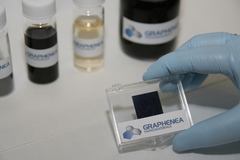
Graphenea is a pioneer graphene production start-up company founded in 2010 by private investors and CIC nanoGUNE. The company produces and commercializes graphene films by Chemical Vapor Deposition technology and graphene powders by Chemical Exfoliation techniques.
ICFO
ICFO is a young research institution located in Barcelona that aims to advance the very limits of knowledge in Photonics, namely the science and technology of harnessing Light. Its research programs target the global forefront of photonics, and aim to tackle important challenges faced by society at large. ICFO is focused on current and future problems in Health, Energy, Information, Safety, Security and caring for the Environment.
IPLEXMED and MindSens winners of the III Global Graphene Call
The London-based MindSens and the Portuguese company IPLEXMED have been selected as the winners of the IIIGlobal Graphene Call, the international initiative aimed at identifying and accelerating business ideas based on the disruptive potential of graphene.
Graphenea embarks on a new era

After the signing of Graphenea’s “declaration of independence”, both parties acknowledge that the expectations raised five years ago have been met, that the mutual collaboration has been excellent, and that Graphenea now has a long and prosperous road ahead of it. Graphenea will continue with the production and commercialization of graphene, and nanoGUNE will continue with its research on the electronic and optical properties of this nanomaterial. Thereby, both entities will continue collaborating in future research projects.
Two years ago, José María Pitarke, nanoGUNE’s Director, declared that the setting up of Graphenea had been "the result of a very high risk gamble," but in which, despite everything, the expectations had been exceeded. This is borne out by the current figures: Graphenea sells its products in nearly 50 countries, has a staff of twelve professionals, and in 2014 its turnover topped nearly one million euros.
Graphene, a material with a future
The outlook is encouraging as graphene production is closely linked to the development of nanotechnology, a world which has only just begun and which has huge potential. Sectors like aerospace, medicine, energy, electronics, etc., companies such as Philips, Nokia, Nissan, and a host of research centers and universities are already using graphene, and many more are expected to do so in the future.
This material, besides being extremely thin (having a thickness of one atom), light (a one m2-sheet weighs 0.77 mg), and strong (about 200 times stronger than steel), has amazing electrical and thermal conductivity, will enable lighter, stronger aircrafts, more efficient light bulbs, better and much longer-lasting batteries, electronic paper, etc. to be produced, and is set to play a key role in future electronics and medicine. According to Pitarke, the advances in nanoscience and nanotechnology constitute the core of current technological development in which graphene has a prominent position.
The setting up of Graphenea was no isolated event, but the result of nanoGUNE's strategy to promote Basque industry, a move made feasible by nanotechnology. Coinciding with the launching of Graphenea, in 2010 nanoGUNE officially opened a nanoincubator (nanoHabia) designed to incubate business projects in the field of nanotechnology. “NanoGUNE’s mission is research excellence for the competitive growth of the Basque Country. To achieve this goal, one of our challenges is to set up new companies" as nanoGUNE’s Director pointed out five years ago. The following companies have been founded by nanoGUNE in addition to Graphenea: Simune (January 2014), which offers atomic-scale simulation services; Ctech-nano (July 2014), which is exploiting nanoGUNE’s capability and experience in atomic-layer deposition in order to offer customized coating services and specific coating tools; and Evolgene (September 2014), whose aim is related to the reconstruction of ultra-efficient ancestral enzymes for applications in a wide range of industrial sectors.
The Nanodevices group participates in the 2D-INK Fet Open project
The Nanodevices group at nanoGUNE is one of the 9 partners of the project. Its contribution will be to fabricate and test transistors with the semiconductor ink provided by other partners in the consortium. NanoGUNE will also take care of the miniaturization of the devices, having in mind possible electronic applications, such as wearables. With this purpose, they will receive 297,600€ for a 3 years period.
The company Graphenea, launched by nanoGUNE and a group of private investors in 2010, will also participate in the project. The collaborative research-team is completed by six more European university partners: Algoritmi Center of the Universidade do Minho (Braga, Portugal); ICMol Institute of the Universitat de Valencia (Valencia, Spain); the Technische Universität München (Munich, Germany); the Katholieke Universiteit Leuven (Leuven, Belgium); the Universität Wien (Vienna, Austria); and the University of Nottingham (United Kingdom).
The FET-OPEN (Future and Emerging Technologies) projects of the European Union support research lines in early stages, based on ideas that may arise new technology lines. Thus, the EU initiative encourages scientists and engineers from many disciplines to cooperate in research projects that promote scientific progress. It is noteworthy, too, that the European program FET -OPEN is a highly competitive call: only 24 of the 643 submitted projects (3.7%) have been funded across Europe.
Patents
The development of semiconductor inks from two-dimensional materials with different properties represent, according to the coordinator of the project, Aurelio Mateo-Alonso, "a major breakthrough in the field of new materials for the next generation of ultra-thin electronic devices such as transistors, LEDs, solar cells, protodetectors, etc.". The researchers also predicts the submission of patents, given the technological possibilities of 2D-INK and the involvement of a private company.
On-chip observation of THz graphene plasmons
Radiation in the terahertz (THz) frequency range is attracting large interest because of its manifold application potential for non-destructive imaging, next-generation wireless communication or sensing. But still, the generating, detecting and controlling of THz radiation faces numerous technological challenges. Particularly, the relatively long wavelengths (from 30 to 300 μm) of THz radiation require solutions for nanoscale integration of THz devices or for nanoscale sensing and imaging applications.
In recent years, graphene plasmonics has become a highly promising platform for shrinking THz waves. It is based on the interaction of light with collective electron oscillations in graphene, giving rise to electromagnetic waves that are called plasmons. The graphene plasmons propagate with strongly reduced wavelength and can concentrate THz fields to subwavelength-scale dimensions, while the plasmons themselves can be controlled electrically.
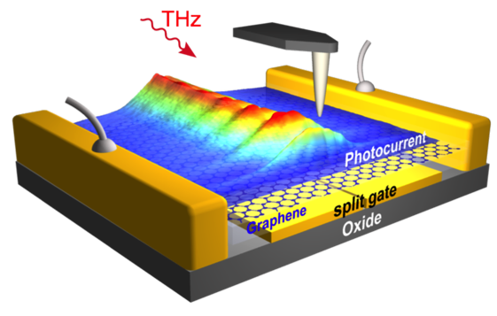
Now, researchers at CIC nanoGUNE (San Sebastian, Spain) in collaboration with ICFO (Barcelona, Spain), IIT (Genova, Italy) - members of the EU Graphene Flagship - Columbia University (New York, USA), Radboud University (Nijmegen, Netherlands), NIM (Tsukuba, Japan) and Neaspec (Martinsried, Germany) could visualize strongly compressed and confined THz plasmons in a room-temperature THz detector based on graphene. To see the plasmons, they recorded a nanoscale map of the photocurrent that the detector produced while a sharp metal tip was scanned across it. The tip had the function to focus the THz illumination to a spot size of about 50 nm, which is about 2000 times smaller than the illumination wavelength. This new imaging technique, named THz photocurrent nanoscopy, provides unprecedented possibilities for characterizing optoelectronic properties at THz frequencies.
The team recorded photocurrent images of the graphene detector, while it was illuminated with THz radiation of around 100 μm wavelength. The images showed photocurrent oscillations revealing that THz plasmons with a more than 50 times reduced wavelength were propagating in the device while producing a photocurrent.
“In the beginning we were quite surprised about the extremely short plasmon wavelength, as THz graphene plasmons are typically much less compressed”, says former nanoGUNE researcher Pablo Alonso, now at the University of Oviedo, and first author of the work. “We managed to solve the puzzle by theoretical studies, which showed that the plasmons couple with the metal gate below the graphene”, he continues. “This coupling leads to an additional compression of the plasmons and an extreme field confinement, which could open the door towards various detector and sensor applications”, adds Rainer Hillenbrand, Ikerbasque Research Professor and Nanooptics Group Leader at nanoGUNE who led the research. The plasmons also show a linear dispersion – that means that their energy is proportional to their momentum - which could be beneficial for information and communication technologies. The team also analysed the lifetime of the THz plasmons, which showed that the damping of THz plasmons is determined by the impurities in the graphene.
THz photocurrent nanoscopy relies on the strong photothermoelectric effect in graphene, which transforms heat generated by THz fields, including that of THz plasmons, into a current. In the future, the strong thermoelectric effect could be also applied for on-chip THz plasmon detection in graphene plasmonic circuits. The technique for THz photocurrent nanoimaging could find further application potential beyond plasmon imaging, for example, for studying the local THz optoelectronic properties of other 2D materials, classical 2D electron gases or semiconductor nanostructures.
Graphenea's new facilities

At the inauguration of the new headquarters of Graphenea have been present the deputy general of Gipuzkoa, Markel Olano, the mayor of Donostia-San Sebastian, Eneko Goia, the director of the company, Jesus de la Fuente, and the director of nanoGUNE, José M Pitarke, among other distinguished guests.
Graphenea was founded in 2010 as part of a joint venture of nanoGUNE with a group of private investors with the purpose of manufacturing and commercializing high quality graphene wafers and developing technologies based on this material. At present, the company based in Donostia is a world leader in the sector, with 14% of the global market share. Its turnover reaches two million euros in a market with a great potential for growth.
The new facilities have required an investment of three million euros, and include a clean room and a pilot plant of graphene oxide that can produce up to one ton of this material per year. Graphenea currently employs 25 people, mostly women.
Contacting the molecular world through graphene nanoribbons
A single molecule can behave as the smallest electronic component of an electronic system. With this premise in mind, researchers in the field of molecular electronics have endeavoured in the last years to develop new approaches that bring closer the long-awaited objective of using molecules as electronic logic components.
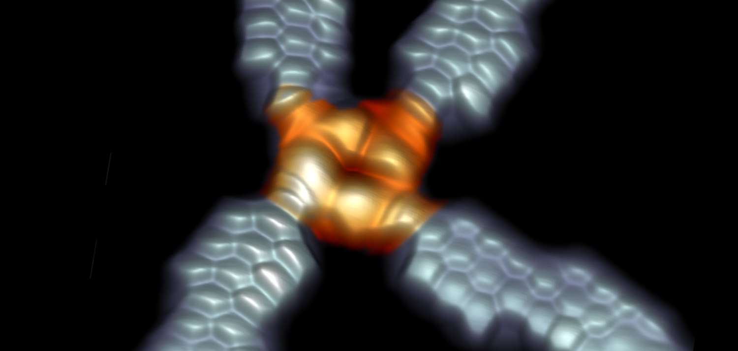
“The idea is fascinating: to store information into a single molecule and read it”, says Nacho Pascual, Ikerbasque Professor and leader of the Nanoimaging Group at nanoGUNE. “We have known for long time how to make the molecules, but we could never wire them into a circuit until now”, he confides. To achieve this goal, scientists developed graphene narrow stripes with the aim of using them as electrical wires; in addition, they also designed a method to precisely contact the molecule at predefined places.
“We found that the contact to the molecule crucially affects how the molecular device behaves”, says Jingcheng Li, first author of the article. “This discovery has made us direct the contacting step with atomic precision technologies”.
Regarding the molecule creation process, researchers have employed in this case a chemical method based on guided chemical reactions over a metallic surface. “The creation of the molecular device is simple”, explains CiQUS team leader, Diego Peña: “we designed and synthetized the building blocks with ‘glue-like’ chemical terminations at the points where contacts are to be created; from then on, nature does the rest of the job for us”, he jokes.
To illustrate the process, this group of scientists has given a very visual metaphor: “we can see it as a molecular LEGO”, they said. In words of Dr. Pascual, “we are learning how to use nature’s laws for assembling molecules into more complex nanostructures”, he claims.
The authors demonstrated the working function of the molecular device using Scanning Tunneling Microscopy (STM), a very advanced method to visualize atoms and molecules, and to measure their behavior. By means of this tool, they could confirm under which conditions the magnetic information stored in the molecule could survive to the contact, opening a new way to develop novel materials for efficient electronics.
The work has been realized in the framework of a Spanish collaborative research consortium named FunMolDev (acronym of Functional Molecular Devices), funded by the Spanish Ministry for the Economy and Competitiveness, the Government of the Basque Autonomous Community, the Xunta de Galicia, and the European Union.
nanoGUNE joins forces with BerriUp and Graphenea to launch the Global Graphene Call
CIC nanoGUNE, BerriUP —a startup accelerator in Donostia— and Graphenea —nanoGUNE’s first startup devoted to the production and commercialization of graphene— have signed a collaboration agreement to drive forward proposals related to research in graphene. So for the first time we are launching the Global Graphene Call designed to develop business ideas linked to graphene.
The participants will need to submit legitimate, in-house projects, and to participate, the project will need to be submitted using the dedicated application form. The starting date for submitting projects is 24 February, 2020 and the deadline is 26 April, 2020.
The shortlisted applicants will be able to take advantage of a programme of customised acceleration at the BerriUp headquarters between June and August 2020, avail themselves of Graphenea material and make use of nanoGUNE’s scientific equipment.
Nature Materials: Graphene plasmons go ballistic
This problem has now been solved, as shown by researchers from ICFO (Barcelona), in a collaboration with nanoGUNE, CNR/Scuola Normale Superiore (Pisa, Italy) – members of the EU Graphene Flagship – and Columbia University (New York, USA).
 Since the discovery of graphene, many other two-dimensional materials have been isolated in the laboratory. One example is boron nitride, a very good insulator. A combination of these two unique two-dimensional materials has provided the solution to the quest for controlling light in tiny circuits and suppression of losses. When graphene is encapsulated in boron nitride, electrons can move ballistically for long distances without scattering, even at room temperature. This new research shows that the graphene/boron nitride material system is also an excellent host for extremely strongly confined light and suppression of plasmon losses.
The research, carried out by ICFO PhD students Achim Woessner and Yuando Gao and postdoctoral fellow Mark Lundeberg, is just the beginning of a series of discoveries on nano-optoelectronic properties of new heterostructures based on combining different kinds of two-dimensional materials. The material heterostructure was first discovered by the researchers at Columbia University.
Ikerbasque Professor Rainer Hillenbrand, nanoGUNE’s Nanooptics group leader, comments: “Now we can squeeze light and at the same time make it propagate over significant distances through nanoscale materials. In the future, low-loss graphene plasmons could make signal processing and computing much faster, and optical sensing more efficient.”
The research team also performed theoretical studies. Marco Polini, from CNR/Scuola Normale Superiore (Pisa) and the IIT Graphene Labs (Genova, Italy), laid down a theory and performed calculations together with their collaborators.
These findings pave the way for extremely miniaturized optical circuits and devices that could be useful for optical and/or biological sensing, information processing or data communications.
Original Publication
A. Woessner,M. B. Lundeberg, Y. Gao, A. Principi, P. Alonso-González, M. Carrega, K. Watanabe, T. Taniguchi, G. Vignale, M. Polini, J. Hone, R. Hillenbrand, and F. H. L. Koppens
Nature Materials (2014) Highly confined low-loss plasmons in graphene–boron nitride heterostructures