Related news by tag Nanofabrication
Basque researchers turn light upside down
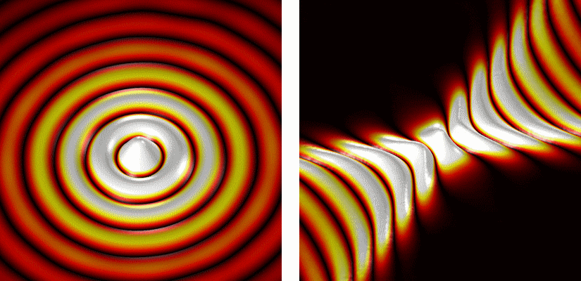
Scientists had already theoretically predicted that specifically structured surfaces can turn the wavefronts of light upside down when it propagates along them. "On such surfaces, called hyberbolic metasurfaces, the waves emitted from a point source propagate only in certain directions and with open (concave) wavefronts", explains Javier Alfaro, PhD student at nanoGUNE and co-author of the paper. These unusual waves are called hyperbolic surface polaritons. Because they propagate only in certain directions, and with wavelengths that are much smaller than that of light in free space or standard waveguides, they could help to miniaturize optical devices for sensing and signal processing.
Now, the researchers developed such a metasurface for infrared light. It is based on boron nitride, a graphene-like 2D material, and was selected because of its capability to manipulate infrared light on extremely small length scales, which could be applied for the development of miniaturized chemical sensors or for heat management in nanoscale optoelectronic devices. On the other hand, the researchers succeeded to directly observe the concave wavefronts with a special optical microscope, which have been elusive so far.
Hyperbolic metasurfaces are challenging to fabricate because an extremely precise structuring on the nanometer scale is required. Irene Dolado, PhD student at nanoGUNE, and Saül Vélez, former postdoctoral researcher at nanoGUNE (now at ETH Zürich) mastered this challenge by electron beam lithography and etching of thin flakes of high-quality boron nitride provided by Kansas State University. "After several optimization steps, we achieved the required precision and obtained grating structures with gap sizes as small as 25 nm”, Dolado says. “The same fabrication methods can also be applied to other materials, which could pave the way to realize artificial metasurface structures with custom-made optical properties”, adds Saül Vélez.
To see how the waves propagate along the metasurface, the researchers used a state-of the-art infrared nanoimaging technique that was pioneered by the nanoptics group at nanoGUNE. They first placed an infrared gold nanorod onto the metasurface. “It plays the role of a stone dropped into water”, says Peining Li. The nanorod concentrates incident infrared light into a tiny spot, which launches waves that then propagate along the metasurface. With the help of a so-called scattering-type scanning near-field microscope (s-SNOM) the researchers imaged the waves. “It was amazing to see the images. They indeed showed the concave curvature of the wavefronts that were propagating away form the gold nanorod, exactly as predicted by theory“, says Rainer Hillenbrand, Ikerbasque Professor at nanoGUNE, who led the work.
The results promise nanostructured 2D materials to become a novel platform for hyberbolic metasurface devices and circuits, and further demonstrate how near-field microscopy can be applied to unveil exotic optical phenomena in anisotropic materials and for verifying new metasurface design principles.
The research has been mainly funded by individual fellowship grants of the European Union Marie Sklodowsca-Curie Actions and the pre-doctoral research grants program of the Basque and Spanish Governments, as well as by the National Science Foundation (USA), and has been carried out in line with nanoGUNEs projects within the EU's Graphene Flagship.
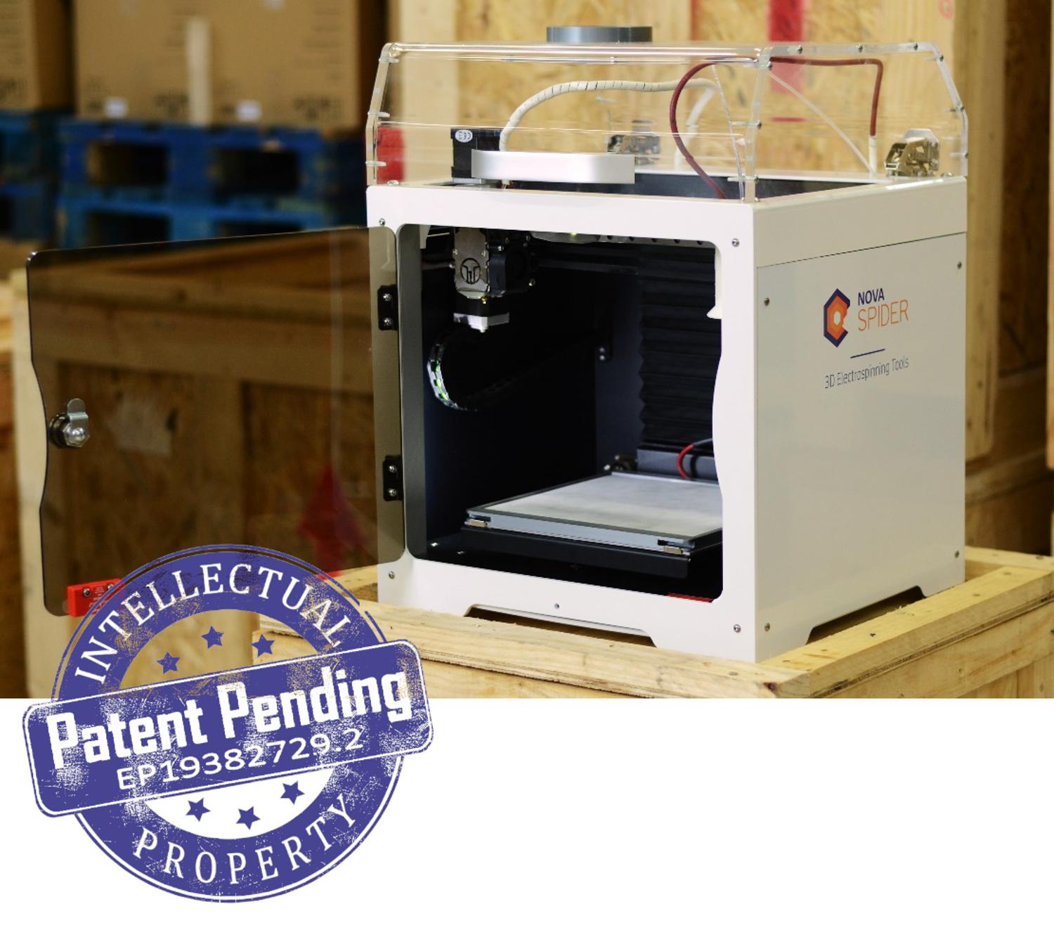
NovaSpider, an innovative technology recently protected through a patent application
The application fields of the structures generated by NovaSpider are versatile and promising. Using polymer nanofibres, whose nature, diameter, appearance and morphology can be modulated in a simple and efficient way, the device allows designing composite materials that are robust, light, porous and offer a high specific surface area. Structures of this type arouse huge interest in regenerative medicine, where they are used as scaffolding in tissue regeneration; in the biomedical sector, where they are functionalized and used in controlled drug release and wound protection; and in the energy sector, where their role as a catalytic converter in superbatteries is being explored.
In turn, it is worth highlighting their application in the textile sector and in packaging, where the idea is to improve the conservation of foodstuffs and to replace plastics by biodegradable materials. To date, the tested sample bank is broad: sugars, proteins, collagen, gelatine, cellulose, etc., thus pointing to the great versatility of the technology. These materials, deposited onto the packaging cardboard, offer a nontoxic and specific barrier between cardboard and foodstuff. The aim is fulfilling the function provided by plastic films until now and substituting them as fully biodegradable coating.
The project is the fruit of the work conducted over the last years by Dr Wiwat Nuansing, an expert in electrospinning, and the engineer Javier Latasa, an expert in mechatronics, among other researchers and technicians in the Self-Assembly Group, led by Dr Alexander Bittner, an Ikerbasque Research Professor at nanoGUNE. The support of experts in the 3D printing industry has enabled the team to meet the highest standards and to include the sector’s latest technological developments.
The NovaSpider equipment integrates FDM/FFF additive printing technology with nanofibre manufacturing techniques involving solvent electrospinning and melt electrospinning:
- FF technology (or FDM: fused deposition material) is a currently very familiar 3D manufacturing process for components with thermoplastics. This method functions by gradually depositing layer upon layer of fused material, which solidifies on cooling to produce the desired object.
- Electrospinning is a technique that consists of subjecting a solution, usually a polymer one, to an electrostatic force produced by the electric field induced when a high voltage is applied between the solution and a grounded collector. This causes a continuous thread to be ejected out of the dissolution in the form of a jet whipping against the collector, from which a nonwoven mat of disordered nanofibres is obtained.
- Melt-electrospinning is a variant of the above. Instead of using solvents, the thermoplastic material is heated until it reaches a liquid state. As in the above technique, an electrostatic force causes a continuous fibre to be extracted from the liquid material. In this case, the fibre usually has a diameter exceeding a micron and follows a straight trajectory, without whipping, from nozzle to collector, which allows its deposition to be accurately controlled, so these microfibre structures can be reproduced by following the desired patterns.