Related news by tag NANOIMAGING
Physicist Nacho Pascual receives ERC Advanced Grant to develop new quantum materials

The prestigious ERC Advanced Grants are the highest recognition of scientific excellence in Europe. They provide long-term funding to support the brightest researchers and their teams while they pursue high-risk, high-benefit innovations in any field of research. The only evaluation criterion required by the European Research Council is the scientific excellence of the project and its research staff, which puts Nacho Pascual at the forefront of European scientific research.
Niklas Friedrich gets GEFES 2023 Award for best experimental thesis
Molecular spintronics is a technology that aims to use the electron spin of organic molecules as the basic unit of information. This thesis studies electronic transport through graphene nanoribbons (GNRs) and demonstrates electronic access to spin states created by special units embedded in GNRs.
A window on the invisible
When working at the atomic scale, matter behaves differently and physics reveals interesting situations. Yet all this entails very important technical requirements. nanoGUNE’s Nanoimaging Group gathers the technical—three huge microscopes— and human resources to put all this into practice.
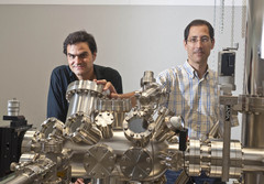
“The properties of materials depend on those of the atoms that form them and on how the atoms are arranged. We aim to research the properties of the atoms individually or in nanostructrues, and to design strategies to assemble them in new materials that optimize their behaviour in a wide range of functionalities like electronics, magnetism or catalysis,” explained José Ignacio Pascual, head of nanoGUNE’s Nanoimaging Group. Some of the applications that could result from the research being done by this group are future electronic devices developed using new materials.
Three in one
José Ignacio Pascual’s research group has designed and built one of their three microscopes. This microscope has the unique capability of measuring electronic, mechanical and optical properties at the atomic scale. The microscope, which has been functioning since January in one of the labs in the basement at nanoGUNE, also allows atoms and molecules to be moved around one by one.
The microscope uses a very sharp tip as a probe to get close to an atom or molecule on a surface and to measure the tunnel current, electrons that jump from the tip to the sample. These electrons fulfil the function performed by light on a larger scale: they allow us to see the atoms and find out their properties.
This microscope operates in extreme temperature and vacuum conditions. That is because at room temperature, atoms have lots of energy and do not stop moving, so it would be impossible to study and manipulate them one by one. That is why Pascual’s group has had to couple the microscope to a tank of liquid helium, a helium cryostat, to work at 269 degrees below zero. The cold temperature is indispensable for keeping the atoms still. And the vacuum is also fundamental to prevent the air, which is also made up of atoms, from distorting the measurements. So work is done with what is known as ultra-high vacuum, 10-13 atmospheres, the equivalent of the intergalactic vacuum.
And it doesn’t stop there. This first microscope is even more unusual. It allows to work with materials that do not conduct electricity, thanks to the fact that José Ignacio Pascual’s group has connected the tip to a small quartz tuning fork. The tuning fork causes this machine not only to work as a tunnel effect microscope, but also as an atomic force microscope. That way the force with which atoms are attracted to each other can be measured, which is essential for studying the hardness of nanomaterials.
Towards electronics of the future
A second tunnel effect microscope, also located in one of nanoGUNE’s labs, works at even lower temperatures: only one degree from absolute zero or, in other words, at 272 degrees below zero. This microscope makes it possible to study problems relating to magnetism in individual atoms. “Atoms are like small magnets whose poles are randomly orientated, and part of our work consists of studying how they are arranged”, said Pascual. “It is an absolutely basic subject of research which has implications in the field of nanotechnology. If we can control the magnetism of atoms one by one, we can reach the limits of matter in the field of information storage. One of the possible applications in the long term would be quantum computing which would allow information to be processed at much higher speeds,” he added.
An adjacent laboratory houses the third atomic force microscope. It is a collaborative tool that “allows to study larger systems that do not require the conditions of cold and vacuum needed to work on individual atoms,” explained Pascual. With this instrument the Nanoimaging group will be contributing its experience in microscopy to the other groups in nanoGUNE, thus expanding its original field of research to the fields of nano-optics, nanomaterials, nanodevices and many, many more.
The work of Pascual’s group is focussing on exploring the fundamental limits of science to spread knowledge and establish the bases for future technology. “What is more, there are technological products directly related with the instruments used in our research and which could be developed here,” added José Ignacio Pascual.
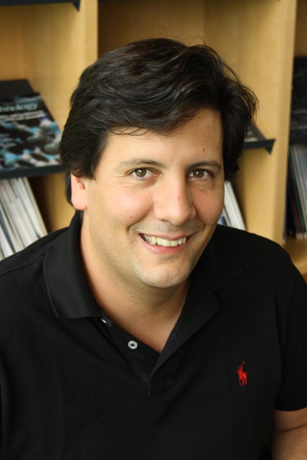
José Ignacio Pascual
José Ignacio Pascual-Chico (Madrid, 1968) is an Ikerbasque Research Professor and leads nanoGUNE’s Nanoimaging group. He has a PhD in Physics from the Autonomous University of Madrid. He was at the Fritz Haber Institute of the Max Planck Society and at the Institute of Materials Science in Barcelona, before arriving in Berlin. He spent a total of 12 years in Berlin, the last eight as Professor at the Freie Universität Berlin. He came to nanoGUNE in September last year to pursue his professional career.
CIC nanoGUNE
The CIC nanoGune Cooperative Research Center located in Donostia-San Sebastian (Basque Country) is a research center set up with the mission to develop basic and applied research in nanoscience and nanotechnology; it does so by encouraging the high level capability and training of researchers in this field, and by fostering cooperation among the various agents in the Basque Science, Technology and Innovation network (universities and R&D centers) and between these agents and industry.
Future materials are becoming 'topological’
Ugeda sees a promising future for materials of this type in spintronics, an emerging branch of electronics that aims to manipulate and control the spin of the electrons in order to use it as a carrier of information. The spin is an intrinsic property of electrons and, unlike its electronic charge, the spin can assume two opposing values: 'up' and 'down'. Therefore, the advantage of making use of the spin is reflected in the increase of the information transmitted. Spintronic devices could transport a greater quantity of data in a much more fluid way with less demand for power and less heat accumulation.
The material explored consists of wolfram and tellurium. Wolfram is a chemical element discovered in 1783 by the Elhuyar brothers in the Basque town of Bergara (Gipuzkoa); it is a metal used in countless applications, ranging from electric lamp filaments to ballpoint pen tips. By combining atoms of this metal with tellurium atoms in just three atomic layers, they discovered the first two-dimensional insulated material with topological properties, in other words, an electrical insulator inside and conductor on its edges. “The flow of electrons along the edges in this type of materials turns out to be linked to the spin (up and down) of each electron; surprisingly, electrons with the opposite spin move in the opposite direction along the edges. So currents with a specific spin in one direction or another can be generated. The channels or grooves along the edge of the material can be imagined as if they were a two-way road in which the “up” electrons go in one direction and the “down" ones in the other. And it cannot be otherwise,” explains Miguel M. Ugeda.
Furthermore, it is worth pointing out that due to the topological properties of this material, the electric current should be insensitive to any contamination and impurities that may be present in the material, a feature that distinguishes topological insulators from conventional conducting materials. Another added advantage is that the material “is chemically stable and relatively easy to synthesize. What is more, it can be combined with other two-dimensional materials in the form of a sandwich in order to design artificial materials with “à la carte” properties for any specific application,” adds the researcher.