Related news by tag Near-field microscopy
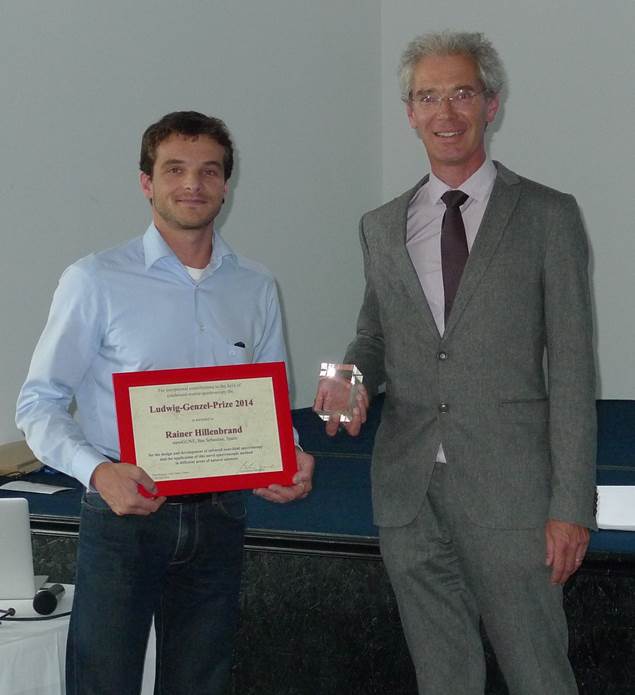
The Ludwig-Genzel-Prize 2014 is awarded to Rainer Hillenbrand
Rainer Hillenbrand received the award from the hands of Prof. Dressel, chairman of the selection committee, during the LEES 2014 conference in Loire Valley (France) for his pioneering and world-leading developments in the field of optical near-field microscopy. Hillenbrand studied at the University of Augsburg and developed his PhD research at the Max-Planck Institute of Biochemistry in Martinsried, both in Germany. During his PhD, Hillenbrand and his colleagues developed a novel scanning near-field optical microscope for background-free amplitude and phase resolved optical imaging with nanoscale spatial resolution, which they named scattering-type scanning near-field microscopy (s-SNOM). This development was a breakthrough in the field and inspired many groups worlwide to start working in this direction. He continued working at the same German institute and built up his own independent junior research group. Further developments made possible to found the start-up company Neaspec in 2007, which has been the first company offering commercial s-SNOM systems.
In 2008, Hillenbrand joined nanoGUNE as the group leader of the Nanooptics group and Ikerbasque Research Professor. He has applied his technique to perform cutting-edge research in different fields, including fundamental solid-state physics, materials science, life science, and nanophotonics. Recent developments include nanoscale infrared Fourier transform spectroscopy (nano-FTIR), which enables infrared spectroscopy with a more than 100 times improved spatial resolution compared to conventional infrared spectroscopy systems. Hillenbrand currently applies the techniques for chemical identification of nanomaterials, protein studies and the development of graphene-based nanophotonics.
According to the price committee, the revolutionary surface-imaging technique allows to perform spectrally resolved measurements from the visible to the microwave regime with an unprecedented spatial resolution. Hillenbrand work “reveals a unique combination of engineering skills and deep insights into the scientific problems of the various topics, addressing both fundamental questions and applications reaching all the way to industrial maturity”.
Ludwig-Genzel-Prize
The Ludwig-Genzel-Prize is awarded to a young scientist for exceptional contributions to the field of condensed-matter spectroscopy. Related to Ludwig Genzel’s scientific oeuvre the focus is on the far-infrared spectral range. The award contains a diploma and prize money of 4000 €. Bruker Optics (Ettlingen) is the sponsor of this prize. The prize is awarded every two years during the International Conference on Low Energy Electrodynamics in Solids (LEES). The selection is made by a committee. The current members of the selection committee are: Martin Dressel —chairman— (Univ. Stuttgart, Germany), Leonardo Degiorgi (EHT Zürich, Switzerland), Jan Petzelt (Academy of Sciences, Praha, Czech Republic), Karl Renk (Univ. Regensburg, Germany) and Hartmut Roskos (Univ. Frankfurt, Germany).
Tracking slow nanolight in natural hyperbolic metamaterial slabs
Hyperbolic materials are very special because they behave like a metal in one direction, but like an insulator in the other. Until now, these materials have been used to fabricate complex nanostructures that permit subwavelength-scale imaging, as well as the focusing and controlling of light at the nanoscale. However, in order to fully exploit their potential, it is necessary to study and understand how light behaves inside them.
The work lays the foundations for studying the precise manner in which light travels through complex optical systems at the subwavelength scale in extremely high levels of detail. Such a capability will be vital for verifying that future nanophotonic devices, perhaps with biosensing or optical computing applications, are functioning as expected.
"The difficulty in performing the reported experiments is the extremely short wavelength of light when it is inside a hyperbolic material” explains Ikerbasque Professor Rainer Hillenbrand, leader of the nanooptics group at nanoGUNE. When light moves inside the material – in our case mid-infrared light in a 135 nm boron nitride slab - it travels in the form of what we call a polariton, where the light is actually coupled to the vibrations of the matter itself".
These polaritons can be considered a double-edged sword to the scientists trying to study them. On the one hand, they squeeze light into much smaller volumes than is normally possible. This is helpful for a wide range of applications that require the manipulation of light in tiny spaces, such as detecting and identifying individual molecules. On the other hand, this ultra-high confinement means that special techniques have to be developed to look at their behavior.
Edward Yoxall, who performed the experiments at nanoGUNE along with Martin Schnell, elaborates: "Because the wavelength of a polariton is so small, we cannot use 'conventional' optical equipment, such as lenses and cameras, to image it. Instead, we have to use a special type of microscope." This microscope - a scattering-type scanning near-field infrared microscope - is capable of seeing details 1000 times smaller than a standard infrared microscope, visualizing "objects" of just 10 nanometers.
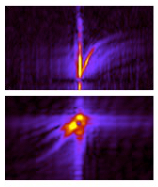
"But it's not just the spatial resolution that makes tracking polaritons tricky", continues Yoxall. "If we want to see how a polariton moves, we need to detect and track it in both space and time. This can be accomplished by using extremely short flashes of light - or pulses- that are just 100 femtoseconds long." That is an extremely small number; less than one millionth of a millionth of a second. By using these very short flashes in combination with their near-field microscope, the researchers are able to watch the polaritons passing different locations along the boron nitride slab, allowing for measuring their speed.
By using both the space and time information that is gathered during the experiment, the scientists have been able to exactly determine how the polariton was travelling. The time- and space-resolved maps revealed a range of intriguing behaviors of the polaritons, including a dramatic slowing down of the pulse velocity - below 1 percent of the light velocity in vacuum- and a reversal of the direction in which the polariton waves were propagating in relation to the direction of the energy flow.
“An exciting result is the speed at which the polariton moves”, says Yoxall. “There’s a lot of interest in slow light, and what we’ve shown here is a novel way of achieving this.” Slow light in conventional photonic structures has great potential for manifold applications in sensing and communication technologies, owing to enhance light-matter interactions. The deep subwavelength-scale confinement of slow polaritons in hyperbolic materials could help to miniaturize these devices.
Basque researchers turn light upside down
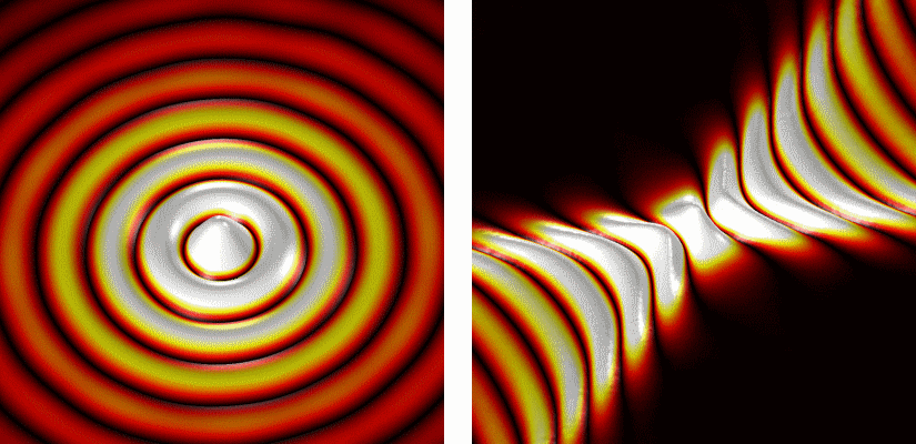
Scientists had already theoretically predicted that specifically structured surfaces can turn the wavefronts of light upside down when it propagates along them. "On such surfaces, called hyberbolic metasurfaces, the waves emitted from a point source propagate only in certain directions and with open (concave) wavefronts", explains Javier Alfaro, PhD student at nanoGUNE and co-author of the paper. These unusual waves are called hyperbolic surface polaritons. Because they propagate only in certain directions, and with wavelengths that are much smaller than that of light in free space or standard waveguides, they could help to miniaturize optical devices for sensing and signal processing.
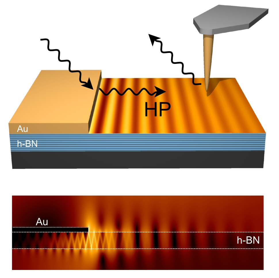
Now, the researchers developed such a metasurface for infrared light. It is based on boron nitride, a graphene-like 2D material, and was selected because of its capability to manipulate infrared light on extremely small length scales, which could be applied for the development of miniaturized chemical sensors or for heat management in nanoscale optoelectronic devices. On the other hand, the researchers succeeded to directly observe the concave wavefronts with a special optical microscope, which have been elusive so far.
Hyperbolic metasurfaces are challenging to fabricate because an extremely precise structuring on the nanometer scale is required. Irene Dolado, PhD student at nanoGUNE, and Saül Vélez, former postdoctoral researcher at nanoGUNE (now at ETH Zürich) mastered this challenge by electron beam lithography and etching of thin flakes of high-quality boron nitride provided by Kansas State University. "After several optimization steps, we achieved the required precision and obtained grating structures with gap sizes as small as 25 nm”, Dolado says. “The same fabrication methods can also be applied to other materials, which could pave the way to realize artificial metasurface structures with custom-made optical properties”, adds Saül Vélez.
To see how the waves propagate along the metasurface, the researchers used a state-of the-art infrared nanoimaging technique that was pioneered by the nanoptics group at nanoGUNE. They first placed an infrared gold nanorod onto the metasurface. “It plays the role of a stone dropped into water”, says Peining Li. The nanorod concentrates incident infrared light into a tiny spot, which launches waves that then propagate along the metasurface. With the help of a so-called scattering-type scanning near-field microscope (s-SNOM) the researchers imaged the waves. “It was amazing to see the images. They indeed showed the concave curvature of the wavefronts that were propagating away form the gold nanorod, exactly as predicted by theory“, says Rainer Hillenbrand, Ikerbasque Professor at nanoGUNE, who led the work.
The results promise nanostructured 2D materials to become a novel platform for hyberbolic metasurface devices and circuits, and further demonstrate how near-field microscopy can be applied to unveil exotic optical phenomena in anisotropic materials and for verifying new metasurface design principles.
The research has been mainly funded by individual fellowship grants of the European Union Marie Sklodowsca-Curie Actions and the pre-doctoral research grants program of the Basque and Spanish Governments, as well as by the National Science Foundation (USA), and has been carried out in line with nanoGUNEs projects within the EU's Graphene Flagship.