New tool for non-invasive quality control of graphene devices
Researchers from the Nanooptics group at CIC nanoGUNE in collaboration with colleagues at ICFO - The Institute of Photonic Sciences (Catalunya) developed a new non-invasive room-temperature technique for graphene device characterization. This work has been funded by the EC Graphene Flagship and was recently reported in Nature Communications.
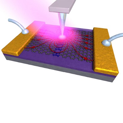
Illustration of the near-field photocurrent technique
nanoGUNE researchers Pablo Alonso González and Ikerbasque Prof. Rainer Hillenbrand, together with ICFO researchers Achim Woessner, Mark B. Lundeberg, Gabriele Navickaite, Davide Janner, ICREA Prof. Valerio Pruneri and ICREA Prof. Frank Koppens (leader oft the international collaboration), developed a noninvasive technique for efficient characterization of the optoelectronic properties of graphene devices at the nanoscale.
Large-scale integration of electronic and optoelectronic graphene devices is becoming a reality. However, to achieve a high device performance, nanoscale and atomic scale imperfections such as grain boundaries, charge density inhomogeneties or additional doping near metal contacts need to be minimized or even eliminated.
The current techniques used for nanoscale graphene device characterization are a major challenge, as most of them are invasive, require specifically designed device structures, can only image small areas, or lack nanometer-scale resolution.
Now, the team of researchers developed infrared photocurrent nanoscopy. This technique combines scanning near-field infrared nanoscopy with electrical read-out, allowing infrared photocurrent mapping at length scales of tens of nanometres. It enables non-invasive and nanoscale probing of the electrical and optical properties of graphene devices at room temperature.
The new technique opens a path for easy, non-invasive and efficient optoelectronic characterization of graphene devices to be integrated in electronic and optoelectronic technologies.