Structural characterization
What we can offer:
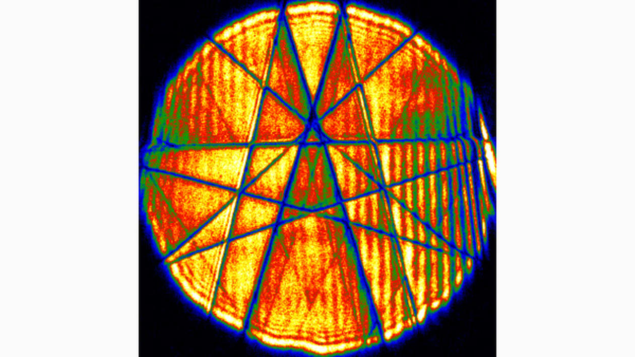
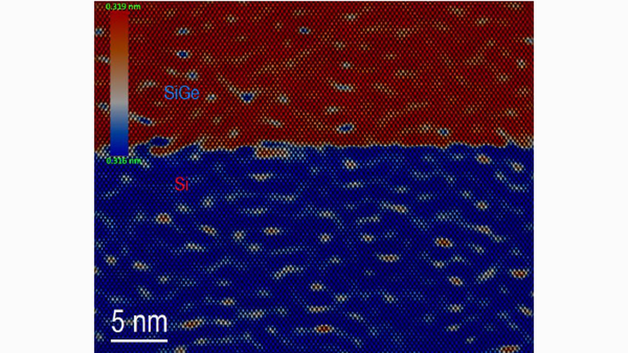
Characterization of materials structure down to the atomic level, nanoscale phase analysis, lattice strain mapping, selected area or convergent beam electron diffraction.
Possibility to:
-
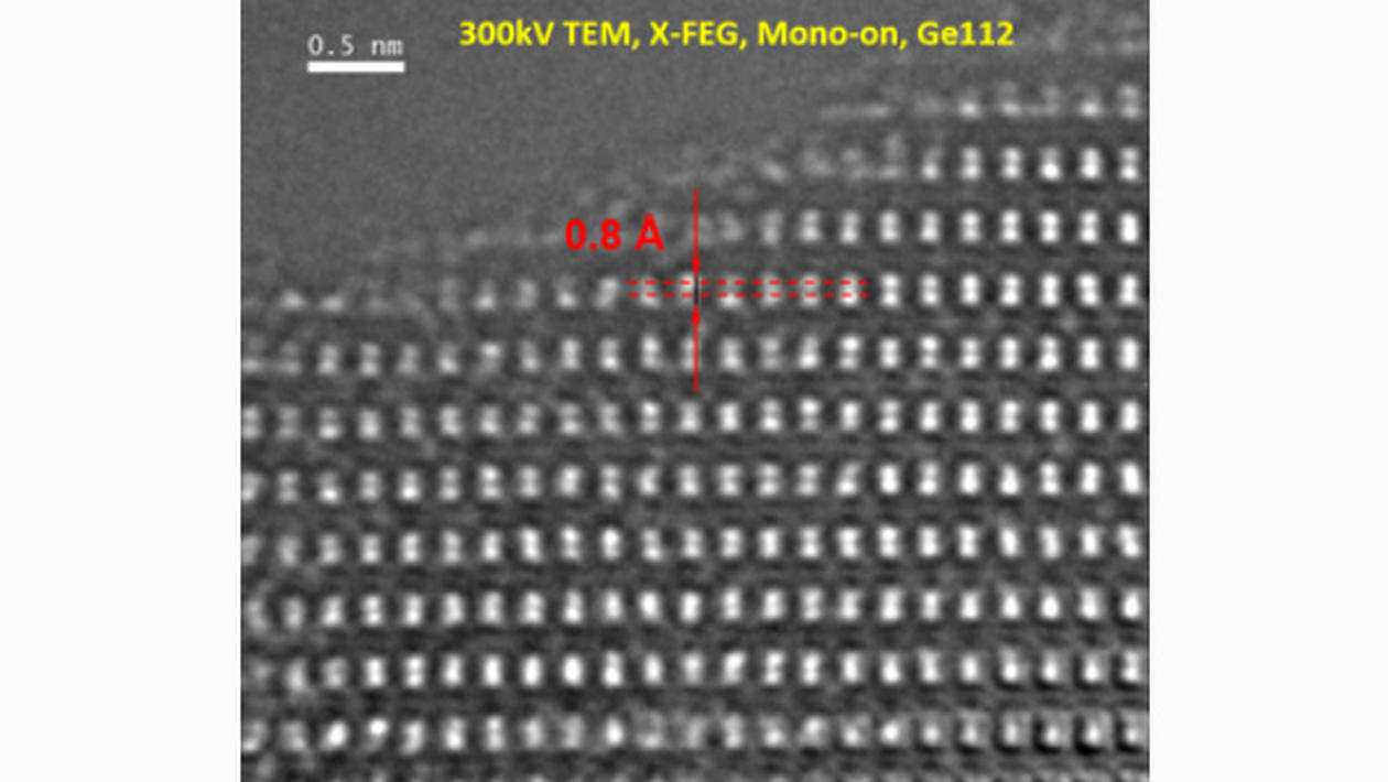
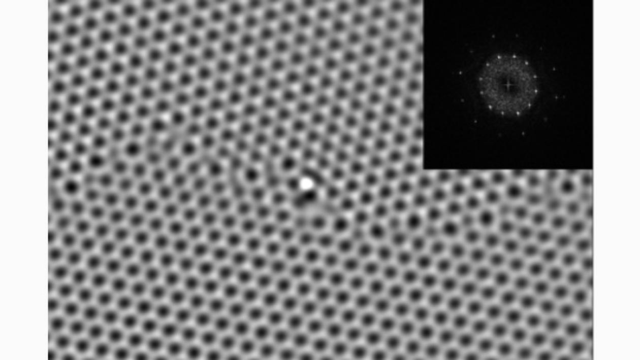
High-resolution TEM/STEM imaging of crystalline or amorphous materials, atomic structure of 2D materials, structure of interfaces and grain boundaries, defects, nanoparticles.
-
Phase identification in inorganic and organic materials: material stress (i.e. SiC, Si), insulator-to-metal transitions (i.e. VO2), polymer crystallinity, mapping of minerals, organic crystals, etc.
Interesting for:
Materials science, microelectronics and semiconductors, automotive, laboratory test facilities, microscopy laboratories, machine-tool manufacturers, iron and steel industry, energy storage and solar-energy materials industry, objects of cultural heritage examination, polymer industry, geology, energy and petrochemical companies.

